Kyocera establishes 3D printing of SiSiC components at the location Selb, Germany
Kyoto/London, 8th July 2025. KYOCERA Fineceramics Europe GmbH has introduced a process for the additive manufacturing of components made of silicon carbide (SiSiC) at its Selb location in Germany. Kyocera is thus expanding its portfolio in the technical high-performance ceramics sector and creating new possibilities for the production of complex, highly resilient components.
“The introduction of additive manufacturing is a milestone for our company,” says Dr Carsten Rußner, President of KYOCERA Fineceramics Europe GmbH. “It brings up new potential for us in terms of development and application as well as strategic positioning in the market.”
3D printing of components made of SiSiC
Silicon-infiltrated silicon carbide (SiSiC) is a high-performance ceramic material with exceptional mechanical strength, thermal conductivity, rigidity and high wear resistance. SiSiC is ideal for demanding areas of application such as aerospace, the semiconductor industry and industrial production, particularly due to its barely measurable thermal expansion. Kyocera processes both StarCeram® Si, which is used for conventional processes, and StarCeram® AM-Si, which was developed for 3D printing, independently – both materials are characterised by comparable material properties.
With the progress of additive manufacturing technologies, 3D printing has proven to be a pioneering method for the production of complex SiSiC components. Compared to traditional shaping processes such as isostatic pressing, slip casting or film casting, additive manufacturing offers significantly greater design freedom and shorter development cycles. For example, topology-optimised components can be produced, which can lead to an enormous reduction in weight. Ceramic 3D printing therefore offers the ideal solution for demanding designs where conventional techniques reach their limits. Thanks to this process, Kyocera offers its customers a broad portfolio of durable, resilient and precise components, from prototype development to series production. The process is generally based on a two-stage procedure: First, a green part is created from silicon carbide powder and polymer binder using the binder jetting process. This is then infiltrated with molten silicon, which reacts with the remaining carbon to form the final SiSiC structure.
“This advancement is the result of intensive research and development work,” explains Sarah Diener, Team Leader for Additive Manufacturing. “We look forward to creating added value for our customers through the production of complex component geometries.”
The advantages of additively manufactured components made of technical ceramics
Complex geometries
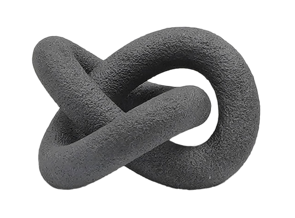
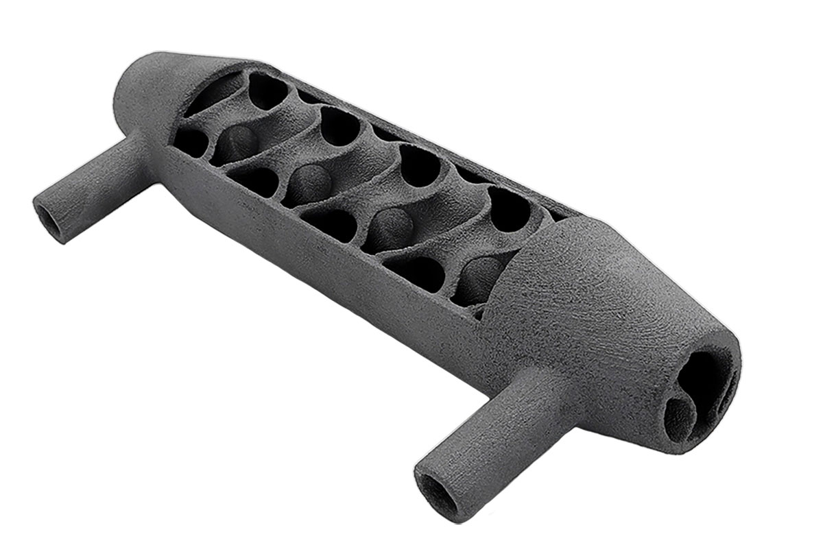
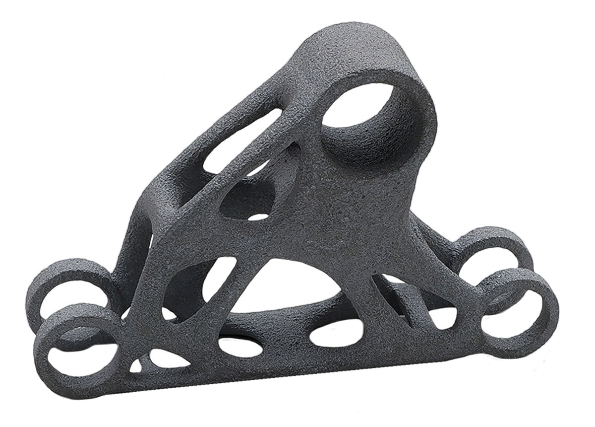
Additive manufacturing enables the implementation of highly complex geometries that cannot be realized using conventional processes. These include curved structures, undercuts and bionic structures. The more complex the geometry, the more the advantages of the process become apparent.
Design consulting
Kyocera offers comprehensive design consulting for the optimisation of component geometries and the implementation of topology-optimised structures. In dialog with the customer, the component weight can be reduced or the performance of the components increased. Thanks to close cooperation with the company's own design centre, tailor-made solutions are created that are optimally adapted to the respective application.
“Additive manufacturing enables us to react flexibly to dynamic market requirements,” emphasises Dr Nikolaos Katsikis, Director Research & Development. “We see great added value for our customers, particularly when it comes to large and complex components – especially when we are able to provide optimisation support through our design consulting.”
Process expertise
With many years of experience in the field of technical ceramics, Kyocera offers not only homogeneous, high-purity materials but also sophisticated post-processing and coating
Examples of complex geometries developed using additive manufacturing from silicon-infiltrated silicon carbide (SiSiC)
technologies that significantly expand the range of applications for 3D-printed components. The location Selb in particular stands out as a comprehensive manufacturer of SiSiC components and is therefore specialised in furnace technology for large-volume components, the final processing of the material, as well as joining experience and coating technologies.
Short production time
The multi-stage production process was specially developed for large-volume and complex components. The maximum component size is 325 x 270 x 130 mm with wall thicknesses from 3 mm. The elimination of green machining, time-consuming programming times and the manufacture of tools for machining enable particularly short production times and the production of large quantities.
With the successful implementation of this technology, Kyocera is underlining its claim to innovation and offering future-proof solutions. The new possibilities not only strengthen competitiveness, but also consolidate the role of the location Selb as a leading centre for ceramic manufacturing technology within the Kyocera Group.