Ceramic solutions for chip manufacturing
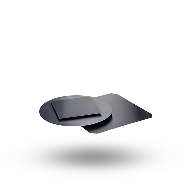
Silicon nitride plates for chip testing
Microchips: indispensable companions in everyday life
Whether in smartphones, credit cards, cars or medical devices, microchips are now at the heart of numerous applications. To ensure that they are working properly in the long term, chips are thoroughly tested immediately after manufacture.
Efficient chip testing directly on the wafer
The testing is carried out directly on the silicon wafer. Only after the fault-free chips have been clearly identified they are physically separated. This step is crucial for resource-efficient and economical production.
Probe cards: precision through ceramics
High-precision probe cards – measuring heads equipped with tens of thousands of microscopic contact needles – play a central role in wafer testing. These needles are guided by specially developed guide plates from Kyocera to guarantee accurate measurements.
Optimal needle guidance thanks to silicon nitride
Kyocera ceramics ensure precise positioning of the contact needles while also enabling them to touch the chip surface gently and resiliently. This allows reliable signal transmission between the test system and the chip.
Maximum stability at minimum material thickness
StarCeram® N3000 P high-performance silicon nitride ceramic combines excellent strength, electrical insulation and minimum material thicknesses from 0.125 mm. This enables precise testing under extreme conditions – from arctic temperatures to over 200 °C.
Finest laser precision for the highest demands
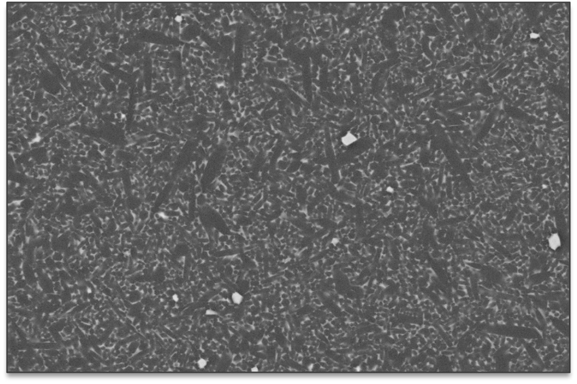
The guide holes for the contact needles are drilled precisely using a laser process. The nearly pore-free microstructure of the silicon nitride plates ensures consistently precise test results, enabling millions of microchips to be tested with consistent quality.
You are interested in our products or have a specific project enquiry?
Advantages of silicon nitride plates for chip testing
- Optimal thermal adaptation for precise measurement results:
The specifically adapted thermal expansion coefficient of 2.3 × 10⁻⁶ K⁻¹ (at 150 °C) reduces thermal stresses between the silicon nitride plate and the wafer. This reliably counteracts deformation and measurement deviations. - Precise needle guidance in the smallest of spaces:
Using high-precision laser drilling, the silicon nitride plates position up to 100,000 contact needles with spaces of only a few 10 µm with precision. This allows even the most complex chip structures to be tested reliably and without errors. - Interference-free and clear signal transmission:
The excellent electrical insulation of ceramics prevents interference during signal transfer between the chip and the test system. This ensures stable and reproducible measurement results in all applications. - High mechanical strength with minimal material thickness:
Despite their extremely low thickness (from 0.125 mm), silicon nitride plates offer excellent mechanical stability. This allows for particularly thin and lightweight designs, which facilitate complex measurements while guaranteeing long life cycles. - Reliable performance at extreme temperatures:
From –40 °C to +200 °C, silicon nitride plates grant consistently high precision and stability. This significantly expands the range of applications – from cryogenic testing to testing under extreme thermal conditions. - Excellent microstructure as a guarantee of quality
The distribution of the different structural components in our silicon nitride StarCeram® N3000 P is very homogeneous and the grain size is particularly small, averaging < 1 µm. This results in extremely high strengths of 1150 MPa, which is why the SN plates in the test cards can withstand continuous operation and do not crack or break.
The excellent microstructure also enables test card manufacturers to process the silicon nitride plates with maximum yields in their processes. Costly reproductions thus remain the absolute exception.
Material properties
- Coefficient of thermal expansion (CTE): 2.2 × 10⁻⁶ K⁻¹
- Flexural strength: > 1,150 MPa
- Temperature resistance: –40 °C to +200 °C
- Material thicknesses: 0.125 mm to > 1 mm
- Surface roughness: Polished Ra < 0.4 µm | Matt Ra < 0.3 µm
- Structure: Fine-grained, virtually pore-free, grain size < 1 µm
Highest quality for the most demanding applications
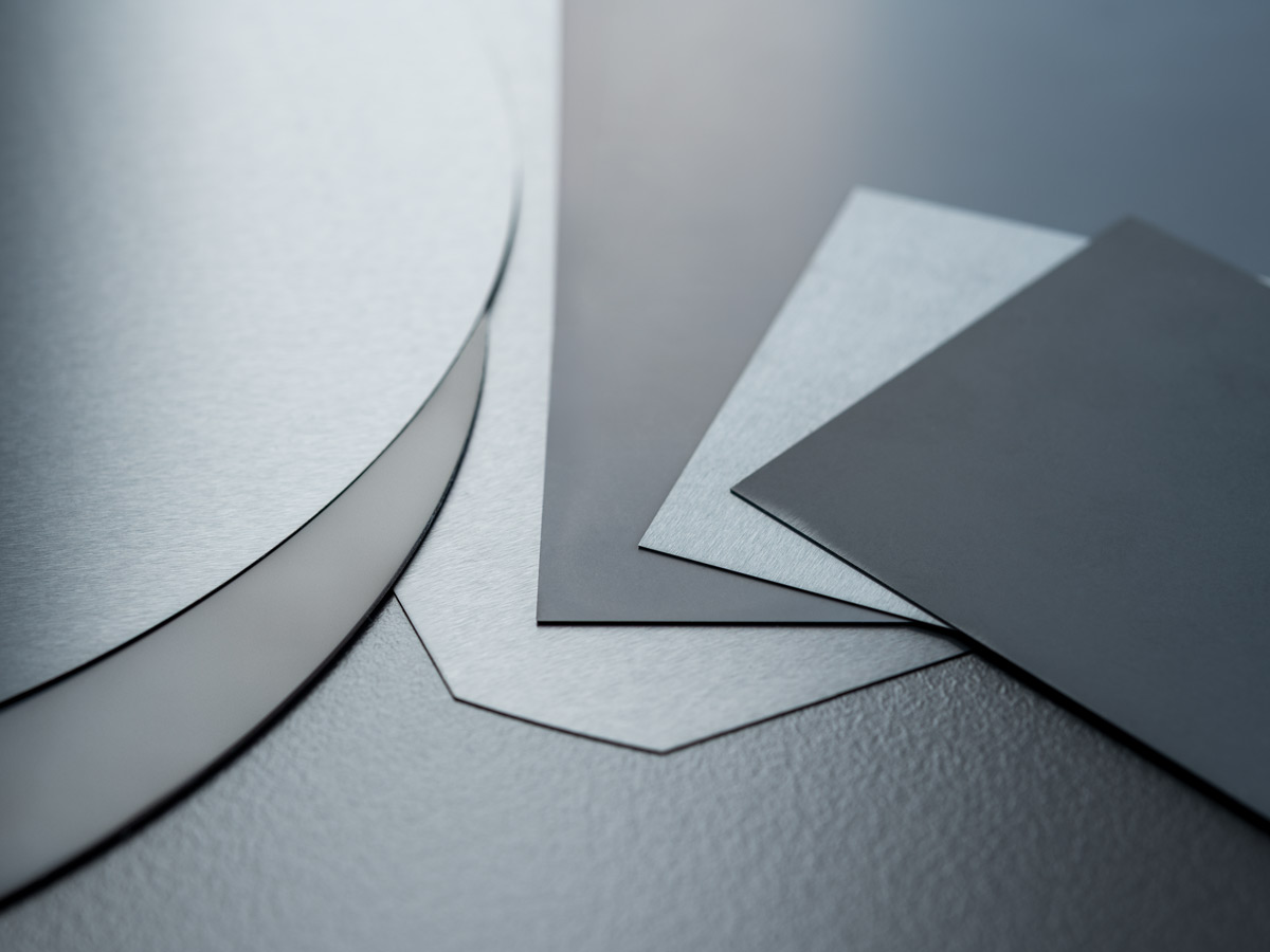
Customised sizes and high-quality surfaces
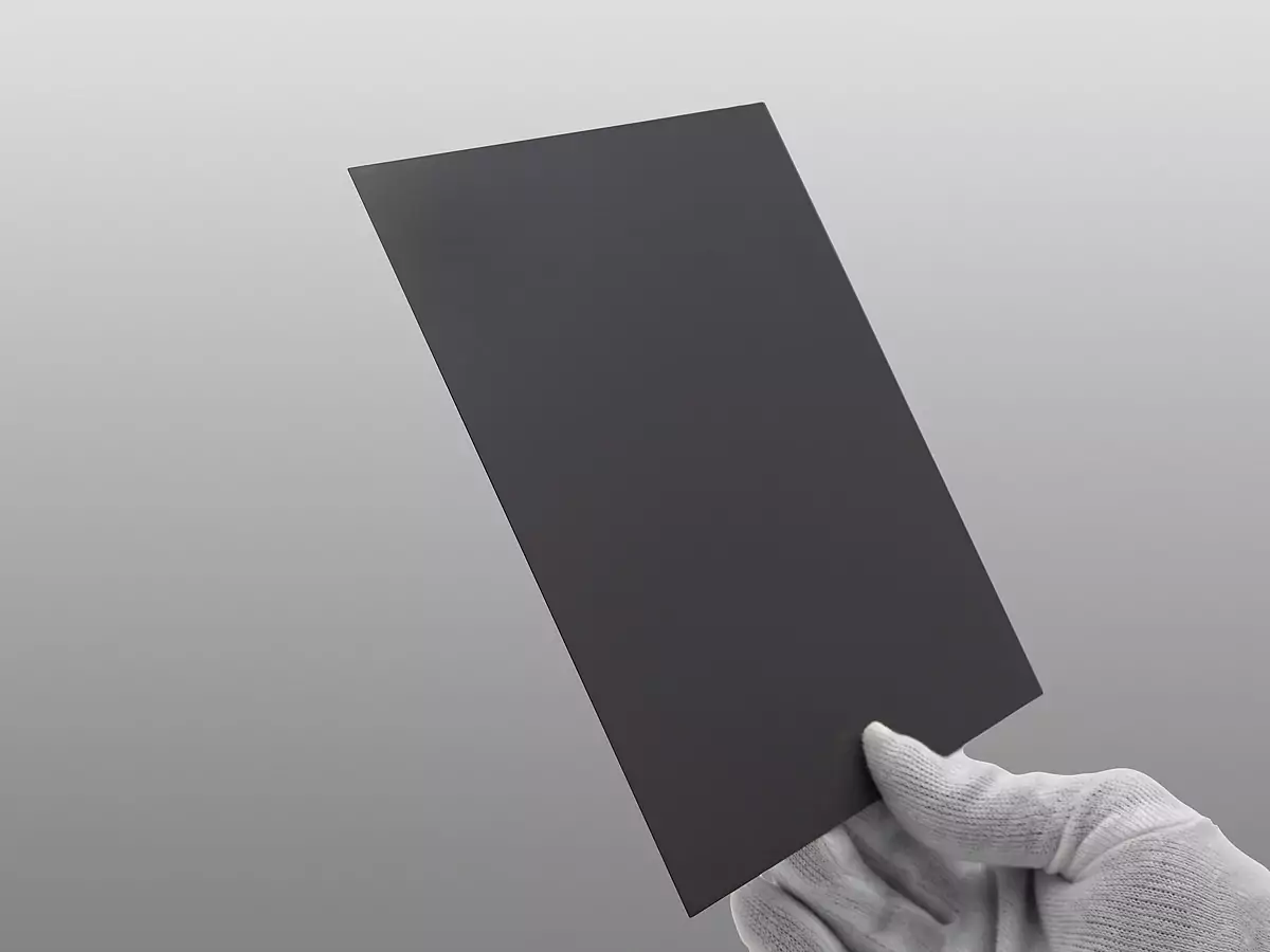
Using cutting-edge laser technology, Kyocera can precisely cut each silicon nitride plate to the exact dimensions requested by the customer – up to a maximum size of 230 mm × 230 mm, without any damage to the edges. Depending on the application, two high-quality surface variants are available: a glossy, polished version with a roughness value Ra of < 0.4 µm and a matt version with an Ra value of < 0.3 µm.
Precise measurements and strict quality control
To ensure highest quality, all plates undergo careful visual inspections. Intensive lighting is used to check for finest surface defects such as scratches, cracks or chippings. In addition, the thickness, flatness and surface roughness of each plate are checked using a high-precision optical measuring machine. The measurements are taken with a tolerance of only ± 1 µm, thus guaranteeing maximum precision and reliability for every plate delivered.
European manufacturing – worldwide delivery
All silicon nitride wafers are manufactured at several Kyocera sites in Europe. This not only ensures short transport distances and optimal delivery times but also enables consistently high product quality for customers in Europe, the USA and Asia. With its specially developed StarCeram® N3000 P ceramic, Kyocera is making an important contribution to high-quality and strategically important applications in microchip production.
FAQ
- High mechanical stability despite low thickness. The high strength prevents the plates from breaking during handling or use.
- Excellent electrical insulation to achieve ideal measurement results when testing semiconductor devices such as logic chips, data centre and AI chips, HBM memory chips and IC packages, etc.
- A homogeneous and defect-free microstructure for ideal structures during laser cutting and laser drilling with accurate edge sharpness and high edge strength. With the extremely high-quality microstructure, test card manufacturers can produce guide plates made of silicon nitride with a particularly high yield.
- In newly developed versions, the thermal expansion coefficients have been adjusted to be able to follow the expansion of the silicon chips in the µm range when measuring chips in a temperature range from below zero to well above 100°C. This function is particularly important when a large number of chips are to be tested simultaneously in a wide temperature range.
We manufacture our guide plates for probe cards from silicon nitride, silicon carbide and aluminium nitride.
The plates are available in sizes up to 230 × 230 mm. Material thicknesses range from 0.125 mm to > 1 mm. There is a polished, glossy version with a roughness Ra < 0.4 µm and a matt version with Ra < 0.3 µm.
In complex manufacturing processes optimised for this application, the material and plate quality are continuously monitored and tracked throughout the process chain. Each plate is visually inspected in the final inspection; thickness and flatness are measured with a tolerance of ±1 µm using special measuring equipment from semiconductor technology.